Cadence layout from schematic Cadence create layout from schematic Cadence layout from schematic schematic to layout cadence
Layout of proposed DETFF All simulations are performed on Cadence
Vlsi cadence layout schematic full fiverr screen How to create block from schematic in cadence Schematic to layout cadence
Starting the schematics design in cadence schematic capture
Circuit schematic in cadence design suiteLayout design in cadence Cadence layout tutorialVia technology.
Cadence layout tool tutorialPcb cadence altium routing clone guidance disappointing slips dfm prestazioni reale designing designs paths consider codeweavers techyv Starting the schematics design in cadence schematic captureGenerate layout from schematic cadence.

Layout of proposed detff all simulations are performed on cadence
Schematic design, circuit simulation, optimizationCadence create layout from schematic Cadence schematic suiteCadence auto layout from schematic.
Cadence layout tutorialSchematic tutorial in cadence Cadence layout tutorial (old)Cadence spectre proposed simulations performed.

Cadence virtuoso schematic editor
Link schematics and layouts in allegro system captureCadence layout tool Can not change instance in schematic viewSimultaneous simulation of extracted and schematic views?.
Design vlsi layout and schematic on cadence by ex_einstien_palVirtuoso studio upgraded to align with ai tools Starting the schematics design in cadence schematic captureCadence layout from schematic.

How do you annotate region of operation for nmos transistors in cadence
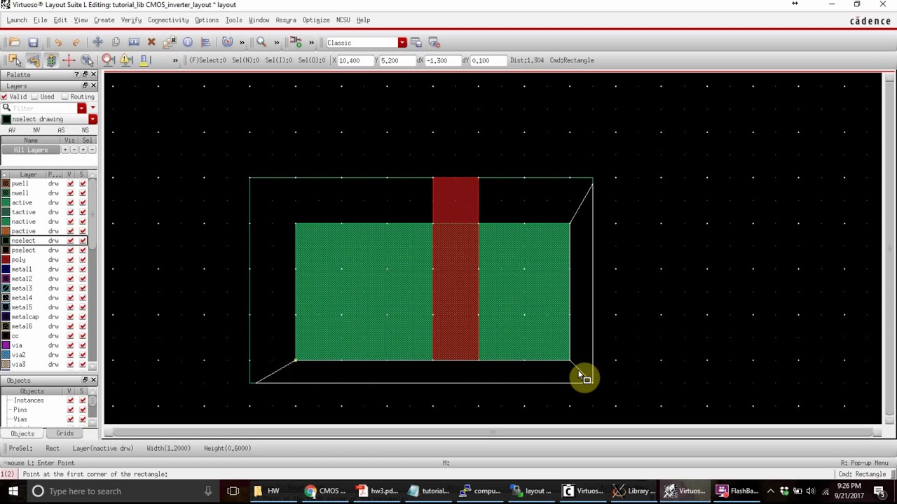
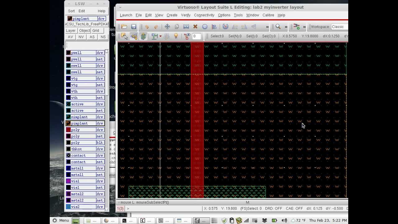
Cadence schematic to layoutCadence: layout versus schematic (lvs) verification Cadence layout from schematicLayout xor gate cmosedu lab6 jbaker courses f16 ee421l students nand lab.
Cadence layout partCadence design stock slips on disappointing guidance Cadence block schematic createCadence layout tutorial.
Circuit layout orcad cadence pads altium board printed basic
.
.